- interfacial energy
Following the treatment given in Sec. III A1 for the interaction energy across the crystalline-amorphous- interface
1. the difference in ⅰ)bulk ⅱ)surface ⅲ)interfacial
energy of {Al2O3}-/2O3>-
2. The stability of the oxide films as a function of growth temperature, oxide filmthickness, crystallographic orientation of
2.3 C-V graph
The measured MOS capacitance (called gate capacitance) varies with the applied gate voltage.
① Measurement of C-V characteristics
-Apply any DC bias, and superimpose a small (15 mV) ac signal
-Generally measured at 1 MHz (high frequency) or at variable frequencies between 1KHz to 1 MHz
-The dc bias VG is slowly varied to get quasi-continuous C-V characteristics
② C-V chara
films were prepared on the ZnO pre-sputtered glass substrate using RF magnetron sputtering system. The PureZnO target was made from high purity ZnO powder (99.99 %) . The MZO/GZO targets were made from high purity ZnO powder (99.99 %) doped with the desired amount of high purity MgO, Ga2O3, powder (99.99 %), respectively. Prior to the deposition, the glass substrates were cleaned using the typica
The threshold voltage of a MOSFET is usually defined as the gate voltage where an inversion layer forms at the interface between the insulating layer (oxide) and the substrate (body) of the transistor. The purpose of the inversion layer's forming is to allow the flow of electrons through the gate-source junction. The voltage of oxide is given by
V_OX= 1/C_OX 2√(qN_A ε_Si V_0 )
SiO_2 V_O
The GZO, MZO thin films were prepared on ZnO pre-sputtered glass substrate using RF Sputtering Technique. Morphological, Structural and Electrical properties of deposited films were investigated in comparison with pure ZnO Thin film by scanning electronic microscopy (SEM), Atomic force microscopy (AFM), X-ray diffraction (XRD), PL spectra and other electrical analytic method. SEM images showed al
1. 실험 목적
본 실험에서는 ZnO(산화아연)의 온도에 따른 결정성의 변화를 XRD를 통해 알아내는 과정에서 X선과 XRD의 정확한 개념의 이해와 XRD 관련 장비 활용 능력을 키워야 한다. 실험의 측정값을 얻은 이후에는 공부한 JCDPS 카드와 다른 이론들을 이용하여 입자의 크기를 구하고 온도에 따른 결정성
서론
1. PDP TV란
- PDP TV(Plasma Display panel TV)는 기존 브라운관 TV와 달리 얇은 유리 기판을 스크린으로 한 TV를 말한다. PDP TV는 Plasma 원리를 이용한 것으로 기판 사이에 혼합 가스를 넣고 높은 전압을 가해 이온가스를 생기게 한 뒤 이를 방전하여 컬러 영상을 만들도록 한다. 이것은 기존 TV에 비해 두께와
For comparative purposes the corresponding peak-to-background ratios were: 4.4, 7.1 and 7.9 for 5kV, 10kV and 15kV, respectively. In addition to Nb, other elemental peaks could be detected from the surrounding materials. The Al and Si peaks were generated from the holder (the O peak was visible due to oxidation of the holder itself), the Ni peak originated from the sample grid and the extraction
도핑 준위
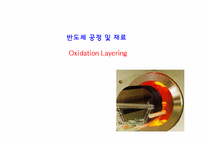
Model : Deal & Grove의 선형-포물선 모델<300 Å - 20,000 Å> 의 성장
150Å까지는 선형적인 산화층의 성장
X = (B/A)t
X : 성장 산화물의 Thickness
B/A : 선형 비례 상수
T : 성장시간
150Å이후는 포물선식 산화층의 성장
X = (Bt)1/2
X = 산화물의 성장 Thickness
B : 포물선 속도 상수
T : 성장시간
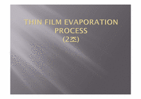
process
Fast deposition speed
Cheap process device
1. Partially different thickness
2. Difficult to control the element ratio
3. Hard to deposition the complex material layer
4. Low film quality
3.Material to be evaporated by e-beam
- E-beam dashes against
material
- E-beam transport energy
to the material
- Then evaporation process
is start